


TSMC, the world’s leading chip foundry, has quietly hit a milestone: volume production of its groundbreaking 2nm (N2) process node is now underway in Q4 2025, right on schedule. This tech leap features first-generation nanosheet transistors using Gate-All-Around (GAA) architecture, ditching the older FinFET design. By wrapping the gate around the channel on all four sides, GAA slashes current leaks, ramps up drive current, and delivers chips that are faster and more power-efficient.
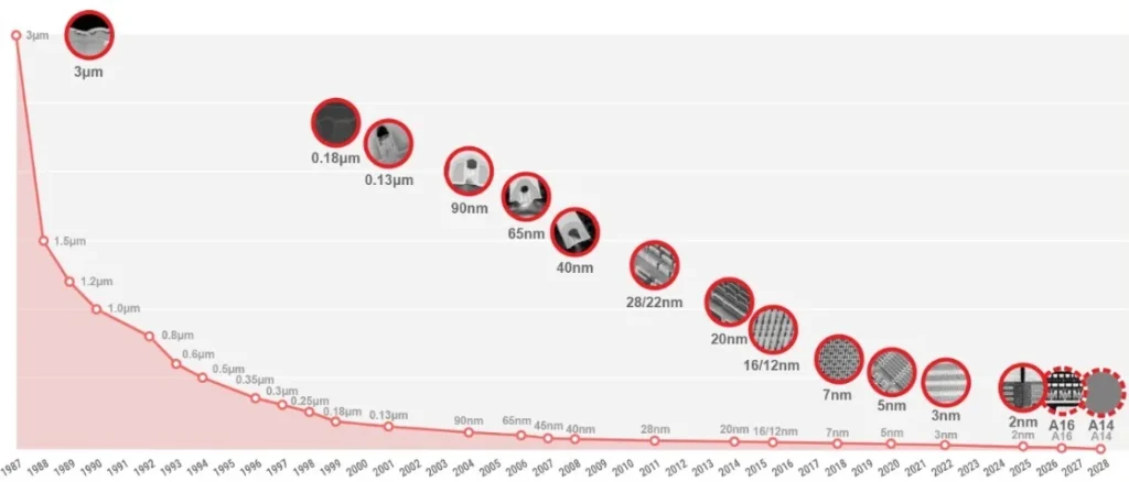
Compared to TSMC’s current 3nm (N3E) node, the 2nm process packs a punch—10-15% faster performance at the same power draw, 25-30% less energy at matched speeds, and 15% higher transistor density for mixed logic, analog, and SRAM designs (20% for pure logic). Transistor density, measured in millions per square millimeter, is the key metric here: smaller nodes mean tinier transistors, fitting more into the same space for superior power and efficiency.
From iPhone 11 to iPhone 18: A Density Explosion
Remember the A13 Bionic in the iPhone 11? It clocked 90-95 million transistors per square millimeter on a 7nm node. Fast-forward to the A17 Pro in the iPhone 15 Pro series—220-290 million on 3nm. Next year’s iPhone 18 Pro Max could debut the 2nm A20 Pro, pushing an estimated 310-330 million transistors per square millimeter. That’s a staggering jump, fueling AI-heavy tasks, longer battery life, and smoother performance.
What’s Next After 2nm?
TSMC isn’t stopping. Expect N2P, an enhanced 2nm variant, in late 2026 with 5-10% better performance. Then comes the A16 (16 Angstrom) node, also slated for H2 2026 volume production. It introduces Super Power Rail (SPR), routing power connections to the wafer’s backside for denser transistor packing and even greater efficiency.
These advancements position TSMC—and by extension, Apple—at the forefront of mobile silicon. As AI demands skyrocket, expect iPhones to handle on-device processing like never before.